 English English |
Deutsch  |
Electron Beam-based Additive Manufacturing
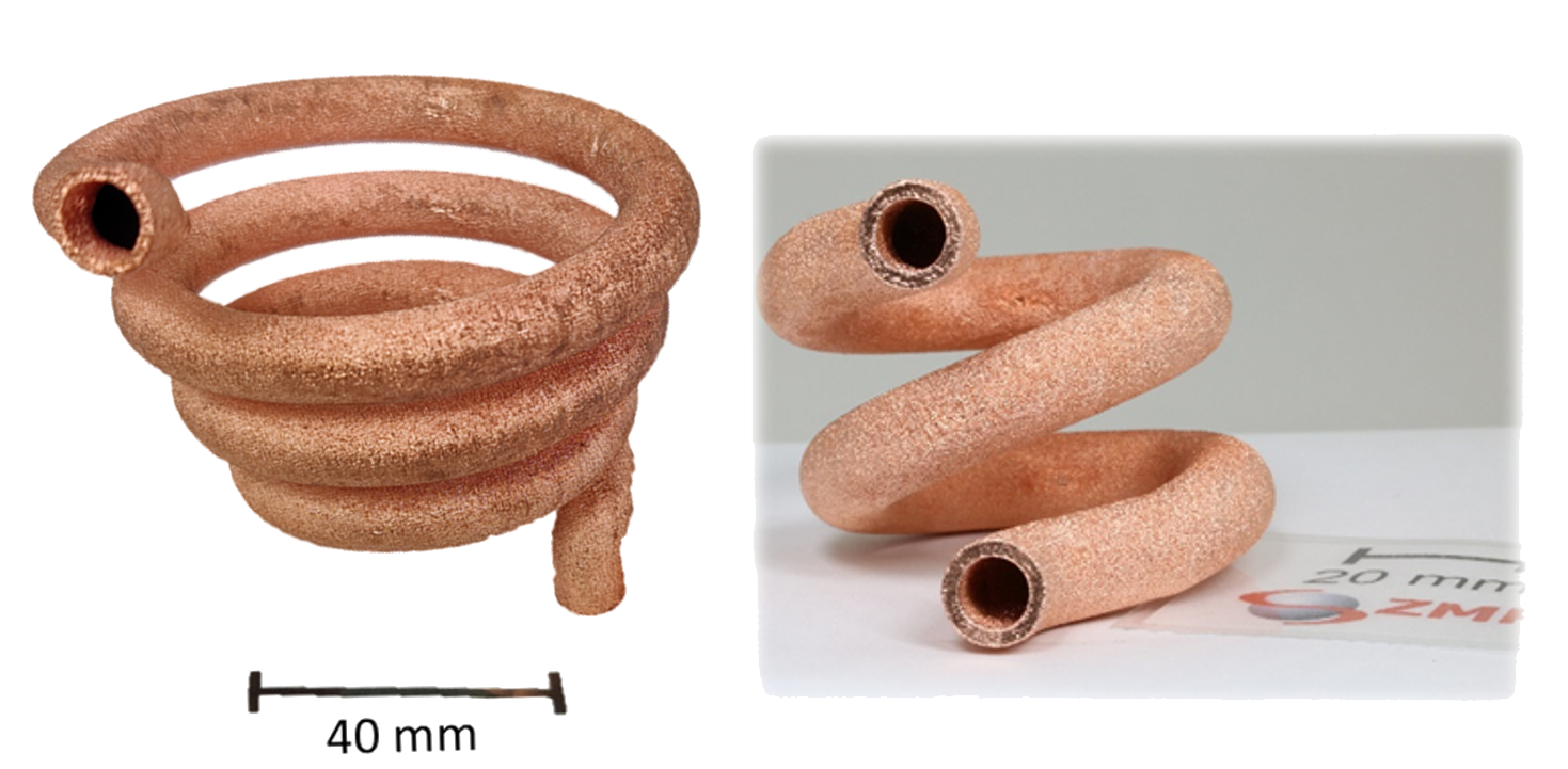
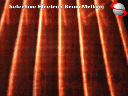
Selective Electron Beam Melting (SEBM) is an additive manufacturing technology. It enables near-net-shaped manufacturing of metals (e.g., titanium alloys, nickel base alloys, titanium aluminide, cobalt chrome or copper, Fig. 1) in almost any geometry. Based on a CAD file, metal powder is melted selectively layer by layer by means of an electron beam generating totally dense metallic components (Fig. 2). Processing under vacuum conditions enables high purity and product quality. Thus, even the processing of materials with a high affinity to gases – which are rather difficult to process under normal conditions – is possible. The resulting material properties are typically in the range of wrought materials.
 |
 |
| Fig. 1: Complex heat exchanger composed of pure copper, manufactured by SEBM. | Fig. 2: Metal powder bed based additive manufacturing by SEBM. |
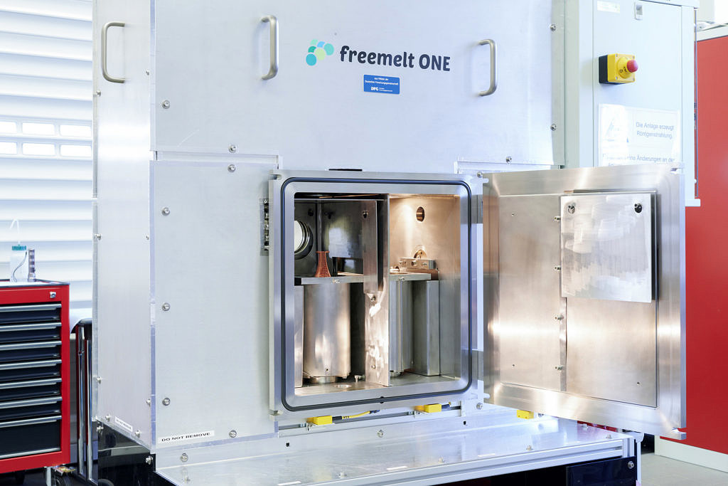
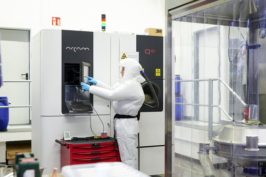
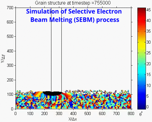
The working group Electron Beam-based Additive Manufacturing addresses the correlation between process parameters, microstructure and the resulting material properties. Currently, numerous SEBM machines are available at ZMP (Fig. 3 and Fig. 4). Suitable process strategies are being developed in order to fully exploit the potential of each material. Process monitoring by means of high speed camera, thermo camera or pyrometer and backscattering electron detector as well as numerical simulation help to gain a comprehensive understanding of the process (Fig. 5).
 |
 |
| Fig. 3: Freely programmable SEBM system Freemelt One (photo taken by David Hartfiel). |
Fig. 4: Mr. Sebastian Wachter is operating the Arcam Q10 SEBM machine (photo taken by David Hartfiel). |
These SEBM machines are being used for the manufacturing of components comprising of compact areas as well as cellular structures (Fig. 6).
 |
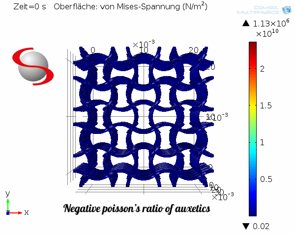 |
| Fig. 5: Simulation of selective electron beam melting of a T-part. | Fig. 6: Simulation of the deformation behavior of an innovative 3D auxetic structure. |
Potential applications are to be found in the field of medical technology, energy technology or automotive sector. Additionally, novel applications in the field of chemical reaction engineering are addressed within our Technology Transfer Center VerTec.